2D Materials and CMOS co-integration at Nanoelectronics Research Group- CITIC-UGR
edited: Carlos Márquez (carlosmg@ugr.es)
About me: C. Márquez
Dr. Carlos Márquez is an Associate Professor in the Department of Electronics at the University of Granada. He earned his B.Sc. degrees in Telecommunications and Electronic Engineering (2012, 2013) and his Ph.D. in Electronics with honors (2017), all from UGR. His research focuses on the design, fabrication, and characterization of advanced solid-state devices for next-generation electronics, with a special emphasis on two-dimensional (2D) materials.
He has authored over 30 peer-reviewed journal papers (including Nature Electronics), five book chapters, and more than 20 international conference contributions, and is co-inventor of two international patents. He has led and participated in European, national, and regional projects, and has been awarded prestigious fellowships, including a Marie Skłodowska-Curie Global Fellowship. He is currently Principal Investigator of the project CMOS-2D-RESET (PID2023-152467OA-I00), focused on CMOS-compatible 2D materials for revolutionary scaled electronics, as well as a related regional project on CMOS-compatible 2D materials for next-generation devices.
Alongside research, Dr. Márquez coordinates undergraduate and master’s courses in electronic engineering, has supervised numerous theses, and actively contributes to scientific outreach initiatives.
About our Materials
2D Materials Overview
Our research focuses on the direct growth of 2D materials such as graphene, MoS₂, and WS₂ using CVD and ALD under CMOS-compatible conditions, and their co-integration at the BEOL to enable scalable, energy-efficient devices for future electronics.

TMDs Fabrication
We use CVD and ALD techniques to fabricate TMDs (WS2 and MoS2) and graphene layered materials.
Processing
Scalable photo-lithography processes are addressed to perform electronic devices.
Characterization
Structural and Electrical characterization give us more details about the quality and thickness of the synthesized materials and about the electrical performance of the devices.
Our Objectives
# 1
2D devices performance
- Fabrication of 2D layered materials
- Structural Characterization
- Processing/Lithography
- Electrical Characterization
# 2
Defect-engineering
- Defect evaluation
- Origin determination
- How to reduce defects implications
- Alternative applications thanks to defects
# 3
Silicon co-integration
- Schottky barrier suppresion
- Metal contacts engineering
- Thermal budget limitation
- Front-gate selection
Latest News
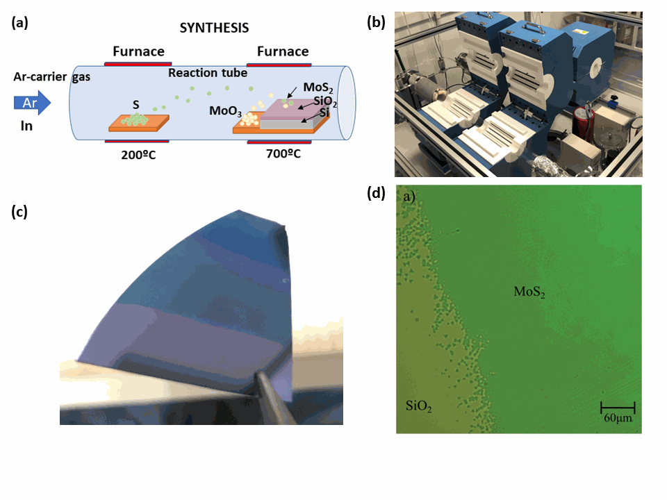
Synthesis of MoS2 layers and other 2D materials
Chemical vapor depositon of MoS2 on SiO2/Si layers. a) Synthesis process in a two-zone CVD furnace. b) CVD furnace PlanarTech. c) Image of the deposited MoS2 layered material on SiO2 sample. d) Optical image.
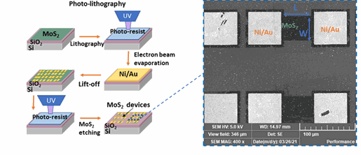
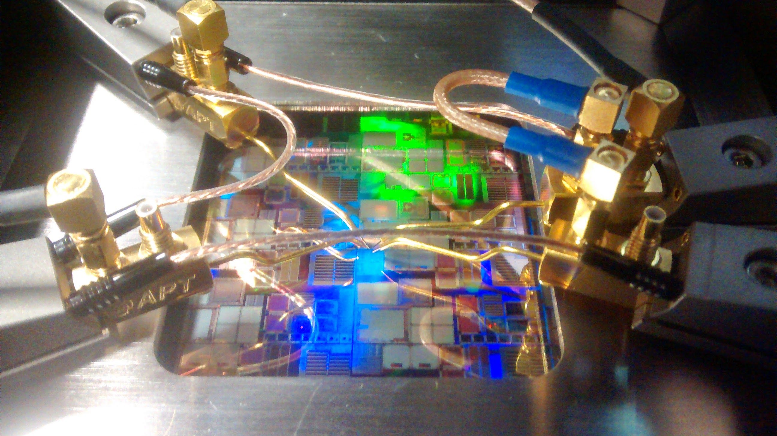
Lithography Process
Optical lithography to perform back-gated devices. Scalable process using standard CMOS photo-lithography. Soruce/drain contactas and MoS2 channel are analyzed in SEM (Tescan Vega 3) image.